
D-Map Cache
Designed, developed and verified a simple Direct Mapped CPU cache for the CFU Proving Ground RISC-V implementation.
TL;DR
Built a simple direct-mapped data cache for the CFU Proving Ground RISC-V SoC in Verilog, sitting between the CPU and main memory. Implemented a 16-line, 64-byte cache with tag/index address slicing, hit/miss handling, CPU stalling, and write-through/write-no-allocate semantics, then verified the design through Verilator simulation and GTKWave debugging while adding cache performance counters to measure hit rates.
Table of Contents
Background
Having gotten extensive practice solving HDLBits and ASMBits problems and reading through Patterson and Hennesy's Computer Organization and Design RISC-V Edition I wanted to get my hands dirty with a project. Exploring different RISC-V implementations I came across Kise Lab's work at Tokyo Insitute of Science on CFU Proving Ground, which with their RVProc RISC-V core gave me the perfect building blocks to add my own hardware component.
CFU Proving Ground in a Nutshell
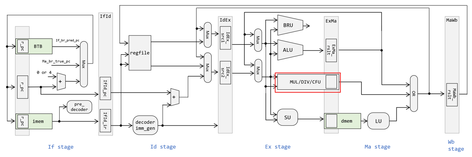
In essence, CFU Proving Ground is an RISC-V acceleration framework for FPGA development which iterates on Google's CFU Playground project. It describes a relatively simple five stage pipelined CPU containing a programmable Custom Function Unit (CFU) allowing users to write their own accelarated instructions using RISC-V's R-type instruction encoding. The diagram below shows the so-called RVProc 32 bit RISC-V core implementation diagram with the actual CFU circled in red.
Beyond the CPU itself, CFU Playground also offers an SoC built from scratch featuring instruction, data, and video memory modules connected via various interfaces and address decoders. It's important to note the entire SoC was is less than 1,000 lines of Verilog code making it extremely compact, readable, and of course extensible ;).
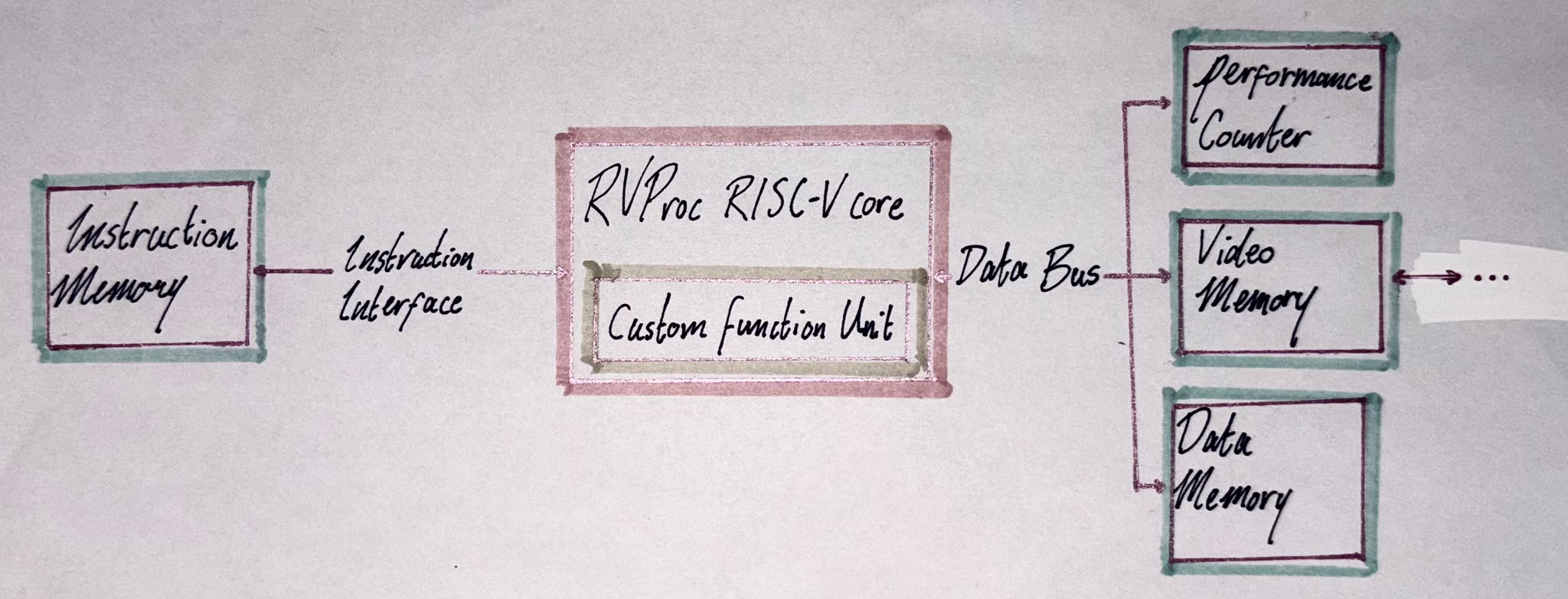
In this SoC diagram the video I/O is truncated as it is not relevant to this project.
main.c file get compiled by GCC and run on a 1,000 line processor feels quite insane!The Plan
Going through the possible extensions of the architecture I considered a handful of options. I thought about extending the existing branch prediction mechanism. Later, I also considered writing a simple UART interface. Finally, I landed on a direct-mapped data cache wich would sit between the CPU and the data memory.
Why specifically a direct-mapped cache?
The cache seemed attractive to me due to it allowing me to study the effect of caching on this particular RISC-V SoC while keeping the implementation simple enough to understand, verify, and modify. Limiting myself to a direct-mapped cache specifically instead of a n-way or fully associative cache made things even more straightforward by not requiring a complex replacement policy. Moreover, I can cover all the data memory with just 16 cachelines containing 32 bit words of data each.
What's the point of adding such a simple cache?
I think this is valid question to ponder. After all, the cacheless CPU has direct access to the memory allowing for lightning fast reads and writes. Adding a cache that uses one or more clock cycles to fetch and store data after a cache miss would effectivly decrease the entire systems performance. Nonetheless, the cache provides me a simplified model of a cached memory hierarchy allowing experiments with temporal and spatial locality. After completing the implementation I would be able to measure the performance impact of cache-aware versus cache-unaware memory-access patterns in (almost) any arbitrary C/C++ code.
The Implementation
Before diving into the code it is important to understand where the cache controller will actually live on the SoC. Unlike some other CPU caches my cache is placed outside of the CPU itself as a standalone module on the SoC as it is fairily simple and externalizing it helps readability. It effectively acts as a proxy between the CPU and the data memory module.
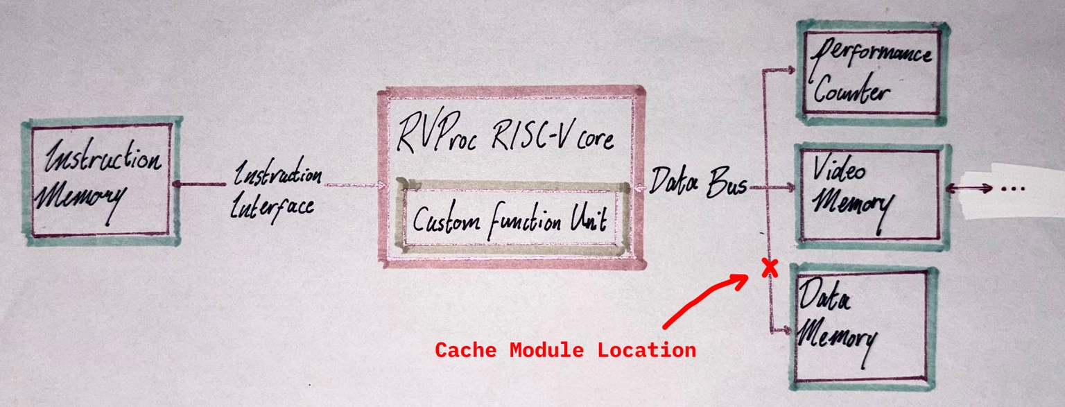
The Interface
As you might expect, this meant that I needed to re-use the current data bus for the CPU to cache connection and create a new bus for communication with the data memory. Both of this should ultimately done without touching any of the CPU/memory internals.
module dmap_cache (
  input  wire        clk_i,
  input  wire        re_i,
  input  wire        we_i,
  input  wire [31:0] addr_i,
  input  wire [31:0] wdata_i,
  input  wire  [3:0] wstrb_i,
  output reg  [31:0] rdata_o,
  output wire        stall_o,

  output wire        mem_re_o,
  output wire        mem_we_o,
  output wire [31:0] mem_addr_o,
  output wire [31:0] mem_wdata_o,
  output wire [3:0]  mem_wstrb_o,
  input  wire [31:0] mem_rdata_i
);
From the CPU side a handful of wires are exposed closely resembling the original memory interface including: re_i and we_i for read/write enable signals, addr_i for the target address, wdata_i for the write data, and rdata_o for the data retruned to the CPU. Also wstrb_i is for requesting bytes and half words through a byte-write mask. The only addition to the interface is the use of a stall output wire stall_o. This wire is simple used to idle the CPU during the cycles when the data is being fetched after a cache miss.
From the memory side things are mostly the same only the direction of the data being reversed.
The Internals
While reading the explanation of the internals keep the following mental model in mind:
From a high-level my cache works like you would expect any CPU cache to work. The CPU requests data, the cache checks whether the data is already present within its storage, if so (hit), it returns the data immediately. In case the data is not present (miss), it asks main memory for the word, stalls the CPU for one cycle, stores the returned word in the appropriate cache line, and then returns it.
Cache Storage
Data is stored within the module in three unpacked arrays of registers:
cache_datarepresents the 16 cachelines containing a 32 bit word each,cache_tagstores the sliced tag of the memory address which is currently associated with the data in the cacheline at one of the 16 indices (more about this slicing in a second),cache_validis initialized at startup to 0 to force compulsory misses when commencing the software boot.
reg [31:0] cache_data  [0:15];
reg [25:0] cache_tag   [0:15];
reg        cache_valid [0:15];
Keeping the cache to just 16 lines meant a tiny hardware footprint which felt right when slotting my module into someone else's SoC. More importantly, a larger cache would yield almost perfect hit rates too easily. A tight 64 byte size intentionally forces cache collisions making the performance difference between cache-aware and cache-unaware code immediately obvious!
Address Slicing
As alluded to earlier, incoming memory addresses requested by the CPU are sliced to determine each memory addresses association within the cache.
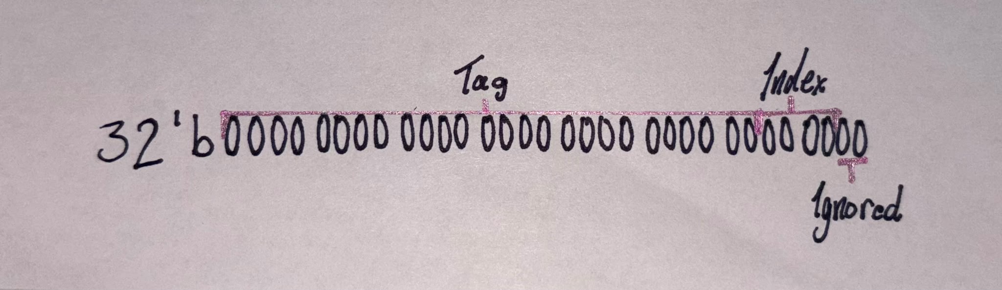
The top 26 bits determine its tag, while the following 4 bits decide which of 16 lines that specific address belongs to.
Written in Verilog it looks like:
index = addr_i[5:2];
tag   = addr_i[31:6];
Now you might have noticed the far right 2 bits, usually meant for byte offsets, are being left unused. This is because the pre-existing byte masking mechanism in the main memory and in the CPU allow my cache to be fully word aligned. No offsets needed!
Hit & Miss Mechanics
Now we get to the heart of the design. To give the cache time to fetch/write data to the memory on a miss I needed to find a way to temporarily stall the CPU. The most elegant approach I could come up with was a relatively simple 2-state finite state machine contained in a combinationalalways block. In essence, the two states represent an IDLE state, where data can immedeatily be written or retrieved, and a WAIT state where the CPU is stalled via its handy stall_i input.
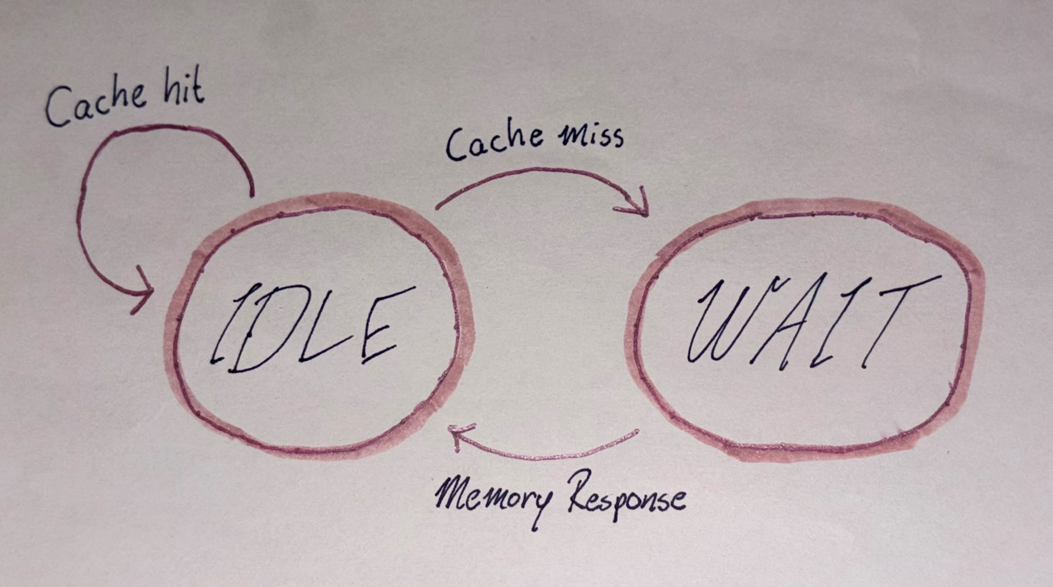
Inside the cache there's a continuously assigned wire called hit which, as you might expect, detects whether the current request matches a hit condition or not. The two simple questions it asks is "Is the incoming index valid?" ('no' here would mean a compulsory miss) and "Does the incoming tag match the current tag in its associated cacheline?".
Read
Perhaps the most straightforward situation is a hit on a read request. In this case the cache simply returns the requested cacheline and that's it!
if (hit) begin
  rdata_o <= cache_data[index];
end
A miss on the other hand temporarily stores the requested index and tag in miss_index and miss_tag vectors. At the same time, the cache's state is switched to WAIT so CPU stalls. One extra cycle is spent fetching data from the main memory after which it is returned back to the CPU and set to the IDLE state again.
Write
The cache uses write-through/write-no-allocate semantics, meaning in this case that writes are always passed along to the main memory whether there's a cache hit or not. So, in practice a write miss doesn't affect the cache's internal storage.
A hit conversely does write to the cache's storage. Importantly, the CPU uses byte strobes to write individual bytes and halfwords. Luckily I didn't have to reinvent the wheel here and I could basically copy the main memory's approach.
if (we_i) begin
  if (hit) begin
    if (wstrb_i[0]) cache_data[index][7:0]   <= wdata_i[7:0];
    if (wstrb_i[1]) cache_data[index][15:8]  <= wdata_i[15:8];
    if (wstrb_i[2]) cache_data[index][23:16] <= wdata_i[23:16];
    if (wstrb_i[3]) cache_data[index][31:24] <= wdata_i[31:24];
  end
  ...
end
if (we_i) begin
  if (wstrb_i[0]) dmem[valid_addr][7:0]   <= wdata_i[7:0];
  if (wstrb_i[1]) dmem[valid_addr][15:8]  <= wdata_i[15:8];
  if (wstrb_i[2]) dmem[valid_addr][23:16] <= wdata_i[23:16];
  if (wstrb_i[3]) dmem[valid_addr][31:24] <= wdata_i[31:24];
end
Testing & Debugging
Perhaps it's important to mention that I did not have access to a physical FPGA board during the development and testing of my cache. Fortunately, the included Makefile already featured some configurations to build and run the hardware in a Verilator emulation.
The default demo program featured in CFU Proving Ground is a simple loop written in C which contiuously prints characters in different colors to random coordinates on a mini LCD display.
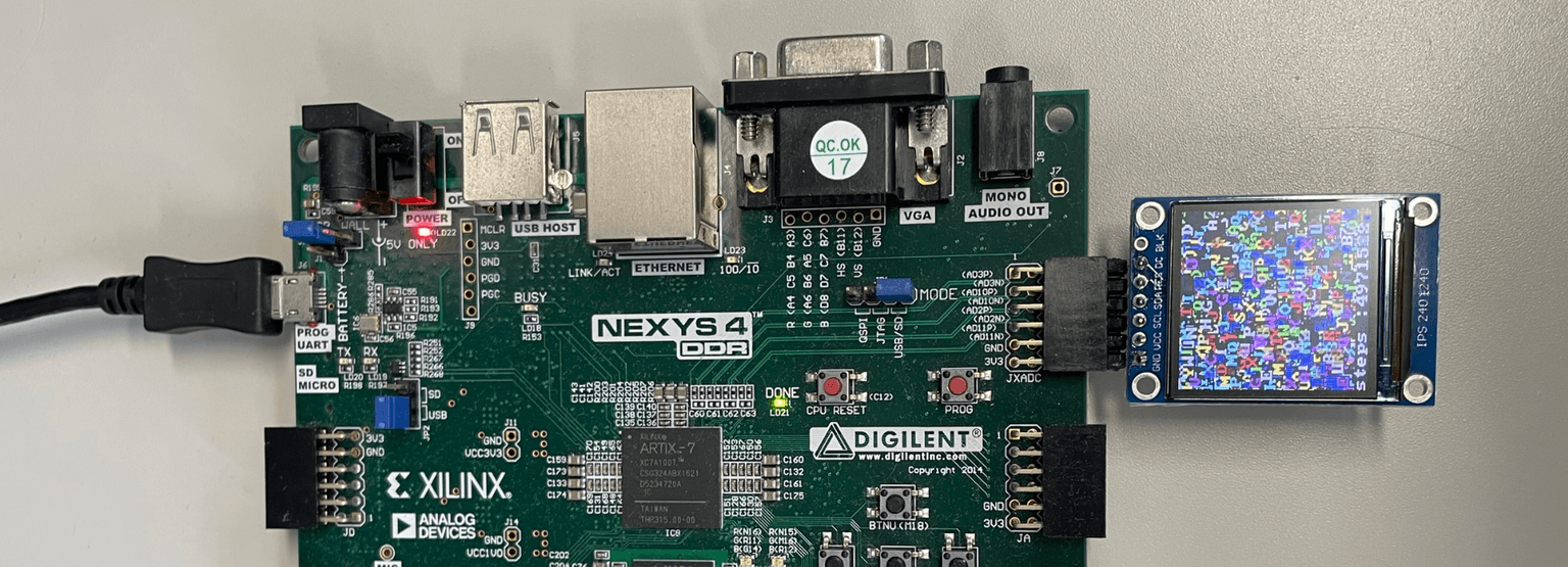
Once again, the Makefile configuration came to the rescue to allow for a connection with a virtual display emulator letting demo the cache on the demo program.
Timing Issue
I was extremely pleased to find out that with only minor compile errors, which I could quickly fix, the SoC succesfully built and was able to run. To my surprise however, I did not see the expected character printing behavior...
| Before Cache | After Cache |
|---|---|
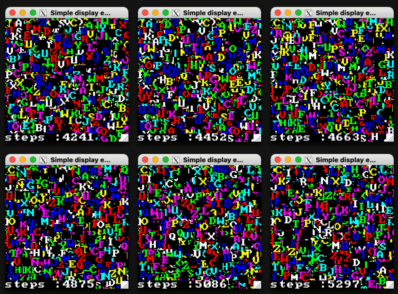 | 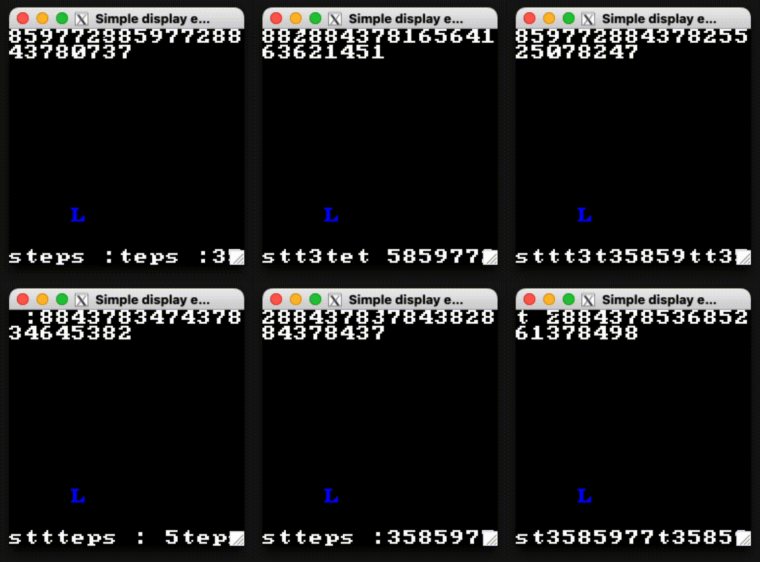 |
This immedeatly screamed timing bug to me. Nevertheless, I was unable to traceback my logical mistake by solely rereading the HDL code. This meant I'd have dive into the signal traces find out exactly what was happening.
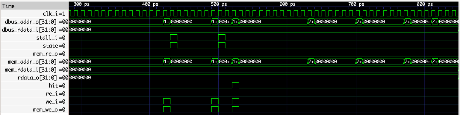
Using GTKWave I managed to find a state (at ~430ps in the screenshot) which reveals the smoking gun! Here we can see that incoming write enable from the CPU we_i is high yet hit stays low, indicating a write miss. As you remember, a miss switches the CPU automatically to the WAIT state which stalls the CPU and writes the incoming mem_rdata_ito its associated cacheline. So what's the problem? This effectivly goes against the write-through/no-write-allocate principle by writing data on a cache write miss. More importantly, the stored mem_rdata_i input from the main memory is most likely not even the value we want to be storing in the first place.
This would explain the "miscalculated" or "unsynced" feeling of the buggy output. The CPU was simply reading stale values it never asked for after write misses. And would you believe it, removing the state switch on write misses resulted an identical character printing animation as the reference.
Measuring Performance
But now we're still left with the question: how do we know whether a given program resulted in a high cache hit rate or not? To answer this I needed to setup some kind of way to have insight into the amount of hits and misses which were ocurring. Firstly, two 64 bit registers are initialized at startup as performance counters respresented as integers.
reg [63:0] cache_access_cnt;    // Total amount of accesses
reg [63:0] cache_hit_cnt;       // Total amount of hits
Why 64 bits? Because we're talking about enormous numbers here. In my SoC design the cache is accessed every other cycle or so. Go figure how many total accesses that amounts to in any program with a decent runtime.
As any rudementary counter, they are simply incremented when the performance condition is met.
if (re_i || we_i) begin
  cache_access_cnt <= cache_access_cnt + 1;
  if (hit) cache_hit_cnt <= cache_hit_cnt + 1;
end
This allowed me to add the metrics to the existing list of Verilator termination logs defined in the top level module of the emulation shell. For a tiny bit more insight I also printed the hit ratio which is just the proportion of hits to accesses.
final begin
  $write("\n");
  $write("===> mcycle                                 : %10d\n", mcycle);
  $write("===> minstret                               : %10d\n", minstret);
  $write("===> Total number of branch predictions     : %10d\n", br_pred_cntr);
  $write("===> Total number of branch mispredictions  : %10d\n", br_misp_cntr);
  $write("===> Total number of cache hits             : %10d\n", m0.cache.cache_hit_cnt);
  $write("===> Total number of cache accesses         : %10d\n", m0.cache.cache_access_cnt);
  $write("===> Cache hit ratio                        : %6.2f%%\n",
    (m0.cache.cache_access_cnt == 0) ? 0.0 :
    100.0 * m0.cache.cache_hit_cnt / m0.cache.cache_access_cnt);
  $write("===> simulation finish!!\n");
  $write("\n");
end
- top.v:47: Verilog $finish

===> mcycle                                 :     614492
===> minstret                               :     581925
===> Total number of branch predictions     :     164858
===> Total number of branch mispredictions  :       7511
===> Total number of cache hits             :      26061
===> Total number of cache accesses         :      26506
===> Cache hit ratio                        :     98.32%
===> simulation finish!!

- S i m u l a t i o n   R e p o r t: Verilator 5.050 2026-07-01
- Verilator: $finish at 6us; walltime 0.118 s; speed 51.972 us/s
- Verilator: cpu 0.117 s on 1 threads; allocated 2 MB
Effects of Cache Aware vs Unaware Code
To make sure both the cache and the performance counters actually make sense let's compare some cache aware C code and compare its metrics to cache unaware code.
Let's take a look at the following example:
int array[64];

int main() {
  int sum = 0;

  for (int i = 0; i < 64; i++)
    array[i] = i;

  for (int k = 0; k < 10000; k++) {
    sum += array[0];
    sum += array[1];
    sum += array[2];
    sum += array[3];
  }

  return sum;
}
The is a textbook example of cache friendly code. The same four elements are accessed repeatedly in a tight loop, meaning that after the initial accesses the cache can serve almost every request directly.
===> Total number of cache hits             :      39996
===> Total number of cache accesses         :      40064
===> Cache hit ratio                        :     99.83%
As expected, the performance counters show a very high hit rate of 99.83%, with only 68 misses out of more than 40,000 accesses.
int array[64];

int main() {
  int sum = 0;

  for (int i = 0; i < 64; i++)
    array[i] = i;

  for (int k = 0; k < 10000; k++) {
    sum += array[0];
    sum += array[16];
    sum += array[32];
    sum += array[48];
  }

  return sum;
}
The second example does pretty much the opposite. By jumping between array[0], array[16], array[32] and array[48], every access maps to the same cache index and continuously evicts the previous value.
===> Total number of branch mispredictions  :          6
===> Total number of cache hits             :          0
===> Total number of cache accesses         :         68
The result is exactly what we'd expect from a tiny direct-mapped cache: 0 cache hits across 68 accesses. This makes the effect of spatial locality (and cache collisions) particularly obvious.